HarmonyOS
Goodix GR551x Series Bluetooth development chips are compatible with OpenHarmony

In January 2022, the Goodix GR551x series – Bluetooth low energy development chips have officially integrated into the OpenHarmony trunk branch. from now, the developer can freely get the source from Gitee.
Last November, the Goodix GR551x series Bluetooth low energy development chips successfully passed the OpenHarmony working’s group compatibility review test and were released in November 2021.
About Goodix GR551x series:
The GR551x series is a high-performance Bluetooth 5.1 System-on-Chip (SoC) that has been widely used in mobile devices, wearables, and Internet of Things (IoT) products. This SoC family is designed to help users develop low-power Bluetooth-based products with a central role and/or a peripheral role.
Moreover, this system-on-chip is well known by the major smart device brand and ODM manufacturers. However, it has exceeded 10 million pieces.
OpenHarmony:
OpenHarmony is the open-source code of the HarmonyOS operating system, which is managed by the OpenAtom foundation and built to help global developers. It has the characteristics of being oriented to all scenarios and distributed.
For source code, visit the below links:
- vendor_goodix: https://gitee.com/openharmony/vendor_goodix
- device_soc_goodix: https://gitee.com/openharmony/device_soc_goodix
- device_board_goodix: https://gitee.com/openharmony/device_board_goodix

Goodix GR551x Series Features:
Bluetooth 5.1 transceiver integrating Controller and Host layers
- Diverse data rates: 1 Mbps, 2 Mbps, Long Range 500 Kbps、Long Range 125 Kbps
- TX power: –20 dBm ~ +8 dBm
- –103 dBm sensitivity( in Long Range 125 Kbps mode)
- –97 dBm sensitivity (in 1 Mbps mode)
- TX current: 3.05 mA @ 0 dBm, 1 Mbps
- RX current: 3.9 mA @ 1 Mbps
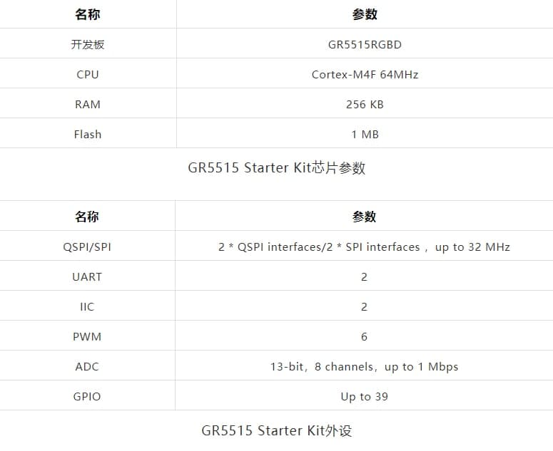
ARM Cortex-M4F 32-bit microprocessor with floating-point support
- Maximum frequency: 64 MHz
- Power consumption: 25 µA/MHz
Memory
- 256 KB RAM
- 8 Mbit Flash
Power Management
- On-chip DC-DC
- On-chip I/O LDO to provide I/O voltage and supply external components
- Supply voltage: 1.7 V ~ 4.35 V
- I/O voltage: 1.8 V ~ 3.6 V
- Ultra-low-power sleep mode with 0.8 µA; no memory retention and wake-on timer
- Light sleep mode: 1 µA, supporting AON_RTC, AON GPIO, and Bluetooth LE Event wakeup
Security
- Complete secure computing engine: AES, HMAC, PKC, TRNG
- Comprehensive security operation mechanism: Secure boot; Encrypted firmware runs directly; eFuse for encrypted Key storage; Application data key is different from firmware key, supporting one secret for one machine
Peripherals
- 2 x QSPI interfaces
- 2 x SPI interfaces
- 2 x I2C interfaces
- 2 x I2S interfaces
- 2 x UART interfaces
- 13-bit ADC, up to 8 channels, up to 1 Msps, supporting both single-ended and differential inputs
- ISO7816 interface
- 6-channel PWM
- Built-in temperature and voltage sensors
- 4 x hardware timers
- 1 x AON hardware timer
- 2 x watchdog timers
- Calendar timer
- Wake-up comparator
- Up to 39 multiplexed GPIO pins
Packages
- 6 mm * 6 mm 48L QFN
- 5.3 mm * 5.3 mm 68L BGA

(Via-ithome)


